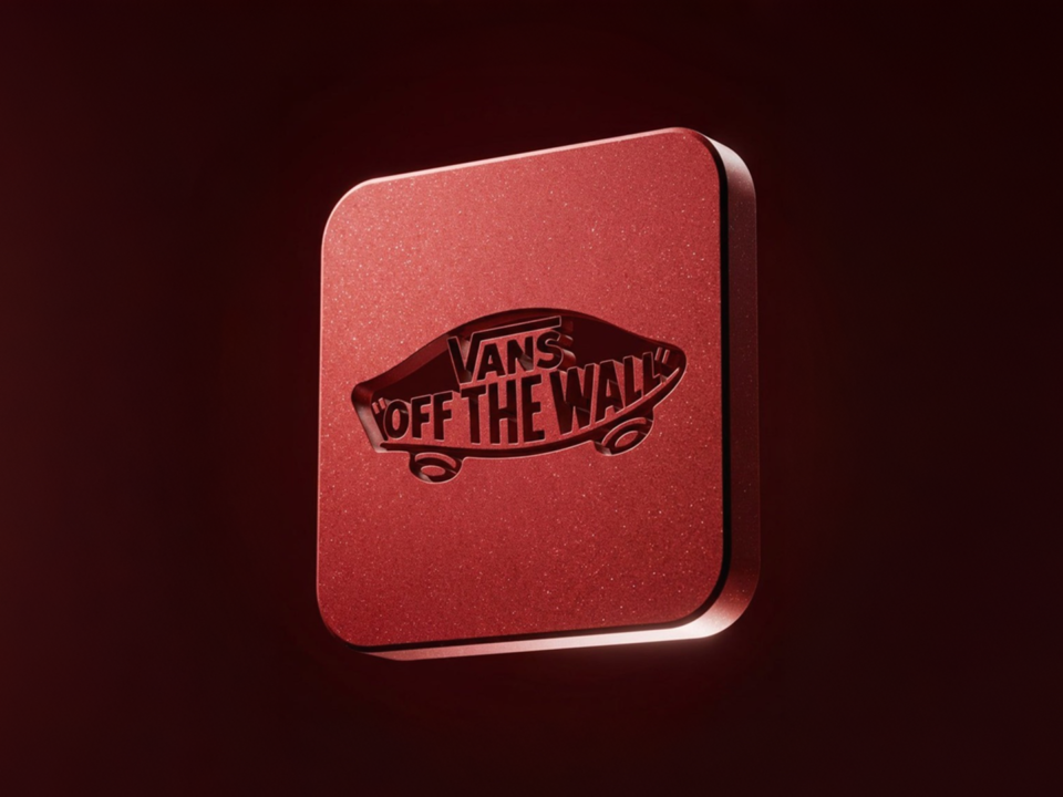
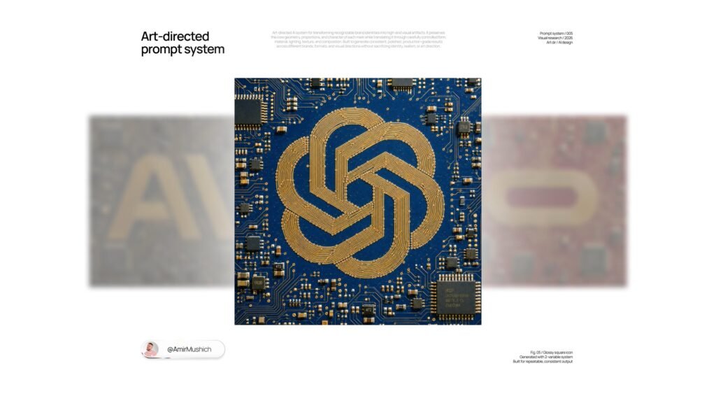
3-variable AI prompt turns any brand logo into a realistic conductive circuit board. Ideal for premium brand design assets.
How to use the prompt
Variables: [BRAND NAME], [METAL MATERIAL], [BACKGROUND COLOR].
Replace [BRAND NAME] with the logo you want (e.g. Apple), [METAL MATERIAL] with the metal (e.g. copper), and [BACKGROUND COLOR] with the PCB color (e.g. green). Then paste the full prompt into GPT Image.
This prompt works great for websites, social media, pitch decks, packaging, or any project that needs polished modern brand visuals.
[BRAND NAME =  _____________]
[METAL MATERIAL = __________]
[BACKGROUND COLOR = _____]

Create a square 1:1 extreme-detail macro visualization of the authentic official standalone symbol of [BRAND NAME], physically fabricated as an intricate conductive circuit-board artwork embedded into a real PCB.

CORE VISUAL SYSTEM

The image must not look like a conventional metallic logo placed on a circuit-board background.

The logo itself must be BUILT FROM the electronic topology.

Translate the authentic geometry of [BRAND NAME] into an extremely dense network of exposed [METAL MATERIAL] conductive traces, contact pads and selectively filled metallic regions integrated directly into a [BACKGROUND COLOR] PCB substrate.

The central visual idea is the collision of two systems:
1. the instantly recognizable authentic brand silhouette;
2. the functional visual language of precision PCB routing.

From normal viewing distance the authentic brand symbol must read immediately. At close inspection, its surfaces and contours must resolve into hundreds of individually routed conductive traces.

BRAND ACCURACY

Automatically identify the most recognizable authentic official standalone symbol of [BRAND NAME].

Preserve its canonical silhouette, proportions, stroke relationships, characteristic curves, intersections, counterforms, internal negative spaces and spacing.

Do not redesign, simplify or replace the identity with a generic symbol.

Ignore the logo's native colors. Translate its geometry exclusively through the PCB and [METAL MATERIAL] material system.

If the official mark contains multiple separated elements, preserve them as separate topological regions with their authentic relative placement.

PCB CONSTRUCTION

Construct the entire image as a physically believable manufactured printed circuit board viewed almost perfectly from above.

The base is a rigid flat PCB covered in a fine matte [BACKGROUND COLOR] solder mask.

The logo is not printed, engraved, embossed or placed on top as a separate solid emblem.

Instead, build its geometry from microscopically raised exposed conductive paths fabricated into the PCB itself.

Use hundreds of narrow [METAL MATERIAL] traces approximately equal in width, with realistic microscopic thickness and softly rounded manufactured edges.

Route neighboring traces as organized parallel streams following the underlying geometry of the brand.

Allow these streams to:
run parallel,
bend around curves,
split,
merge visually without physically intersecting,
change direction,
compress in narrow areas,
expand across broad areas,
and flow around authentic negative spaces.

Use PCB-like angular routing where appropriate, including restrained 45-degree directional transitions, but allow smoother routing where required to preserve characteristic brand curves.

The topology must feel deliberately engineered rather than generated as random decorative circuitry.

TRACE LANGUAGE

Treat conductive traces like extremely precise contour drawing.

Use trace direction to describe form.

Broad logo regions should contain long families of parallel traces.
Curved regions should create controlled nested contour flows.
Tight intersections should produce denser routing.
Negative spaces must remain clearly open and readable.
Outer boundaries should be resolved by the termination and direction of traces rather than by one heavy decorative outline.

Vary topology locally while maintaining one coherent manufacturing language.

Do not fill every region with identical circuitry.

Where useful for visual hierarchy, allow selected important regions to become continuous exposed [METAL MATERIAL] planes surrounded by dense routed traces, similar to large copper pours on a PCB.

These solid metallic areas should remain shallow and flush-to-slightly-raised, never becoming thick 3D extrusions.

ELECTRONIC ENVIRONMENT

Surround the central brand artwork with authentic miniature PCB architecture extending naturally toward all frame edges.

Include realistically scaled:
SMD resistors,
ceramic capacitors,
small IC packages,
microchips,
IC pins,
contact pads,
vias,
solder joints,
small rectangular electronic components,
and dense secondary conductive routing.

Arrange components in believable engineered clusters.

Some traces from the logo may visually continue toward surrounding circuitry so the brand appears genuinely integrated into the electronic system rather than pasted into its center.

Maintain irregular but intentional component density. Leave occasional calm areas of exposed solder mask between dense electronic clusters.

Do not create random sci-fi circuitry, glowing technology patterns or decorative motherboard graphics.

METAL MATERIAL

All exposed conductive artwork uses [METAL MATERIAL].

Treat [METAL MATERIAL] as a physically real conductive surface with its authentic optical behavior rather than simply assigning it a color.

The traces have microscopic rounded shoulders and extremely small edge radii that catch narrow highlights.

Use restrained surface micro-texture and minute manufacturing variation.

Metallic planes should show a subtle fine-grain finish rather than perfectly smooth CGI surfaces.

The material should produce:
soft broad reflections on larger exposed regions,
thin bright specular lines along microscopic trace edges,
subtle tonal variation between neighboring traces,
and darker reflected values where the environment is blocked.

Avoid chrome-like perfection unless [METAL MATERIAL] physically requires it.

PCB MATERIAL

The [BACKGROUND COLOR] PCB solder mask is deep, dense and predominantly matte with subtle low-level reflectivity.

Add extremely fine physical grain, microscopic manufacturing texture and occasional tiny surface imperfections visible only at macro scale.

Keep the substrate visually quiet so the metallic routing remains dominant.

No stone, plastic slab, fabric, painted panel or generic colored background.

[BACKGROUND COLOR] must describe the actual PCB solder-mask color.

MICRO-RELIEF AND CONTACT

The metal traces sit only microscopically above the solder-mask surface.

Create tiny contact shadows and restrained ambient occlusion immediately beside raised conductive paths, pads and components.

The relief must be tactile under macro photography but physically shallow.

Do not turn traces into thick wires, tubes, cables, ropes or extruded typography.

Solder joints should show tiny convex metallic menisci where components meet pads.

Component bodies should have realistic ceramic, polymer and semiconductor-package roughness distinct from the conductive metal.

LIGHTING

Use controlled macro product-photography lighting.

Place one very large diffused rectangular softbox above and slightly upper-left/front of the PCB, broad enough to illuminate the complete scene consistently.

Its reflection should create soft luminous bands across large metallic areas and thousands of coordinated narrow highlights along the raised conductive traces.

Use weak neutral frontal fill only to prevent black clipping.

Maintain enough negative fill that microscopic dark separation remains visible between neighboring traces.

The lighting must reveal the physical height and curvature of the circuitry through grazing specular response and micro-shadowing.

No colored rim lights.
No neon.
No emissive circuitry.
No artificial glow.
No dramatic volumetric light.

REFLECTION SYSTEM

Reflections are essential to describing the micro-geometry.

Each metallic trace should carry a narrow controlled specular response generated by the same large studio source.

Highlights should vary naturally as traces change orientation.

Long parallel traces should create rhythmic families of coordinated bright and dark lines.

Curved routing should visibly bend the reflections with its geometry.

Larger metallic regions should carry broader softbox reflections with smooth tonal falloff.

Avoid uniformly bright gold outlines or identical highlights on every trace.

CAMERA

Photograph the PCB almost perfectly perpendicular to its surface.

Use the visual character of a 90–120 mm macro or telephoto product lens.

Camera pitch and yaw approximately 0–2 degrees.

Minimal perspective convergence and minimal geometric distortion.

The result should feel nearly orthographic while retaining the subtle optical character of real macro photography.

Frame the authentic brand symbol prominently in the center while allowing surrounding electronics to crop naturally against all four edges.

The board itself extends beyond the image boundaries.

DEPTH OF FIELD

Keep the central PCB artwork and almost all of the logo sharply resolved.

Use approximately f/8–f/11 macro-product-photography behavior.

Only extremely subtle optical softening may appear toward distant peripheral micro-components.

Do not use shallow cinematic macro blur or strong bokeh.

Every important conductive trace inside the brand symbol must remain individually legible.

RENDER CHARACTER

Create the physical credibility of an exceptionally detailed photographed custom PCB.

Use physically based path-traced material behavior, realistic micro-specular response, restrained ambient occlusion, accurate metallic reflections, microscopic edge rounding, subtle surface roughness and high-frequency manufacturing detail.

Preserve tiny imperfections that prevent the object from feeling procedurally perfect.

The final hierarchy must read at three distances:

DISTANCE 1 — unmistakable authentic [BRAND NAME] symbol.

DISTANCE 2 — sophisticated flowing architecture of parallel [METAL MATERIAL] conductive traces.

DISTANCE 3 — real PCB fabrication detail: microscopic pads, solder, vias, component surfaces, edge reflections and material grain.

NEGATIVE CONSTRAINTS

No conventional solid 3D logo.
No logo floating above the PCB.
No backing plate behind the logo.
No printed logo.
No engraved logo.
No thick metallic extrusion.
No thick wires or tubular circuitry.
No generic circuit texture clipped inside a logo mask.
No random maze pattern.
No cyberpunk styling.
No neon.
No glowing traces.
No holographic effects.
No futuristic HUD graphics.
No excessive bloom.
No dramatic shallow DOF.
No wide-angle perspective.
No perfectly clean synthetic surfaces.
No ornamental circuitry unrelated to the authentic brand geometry.

The circuitry must define the identity itself: authentic brand geometry reconstructed through physically plausible PCB routing and [METAL MATERIAL] fabrication.